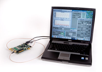
LLRF4.6 Evaluation Board
 The LLRF4.6 evaluation board is designed for RF signal processing with accelerator low-level RF as the primary application. Four input channels are sampled by high-speed high-resolution ADCs, optimized for IF sampling. The channels include IF bandpass filtering as well as provisions for on-board RF-to-IF downconversion. The board is populated with four Linear Technology LTC2255 14-bit 125 MSPS ADCs. At the back-end two DAC channels are available, implemented using Intersil ISL5927 - a dual 14-bit 260 MSPS device. Back-end channels can be configured for direct IF output or IF-to-RF upconversion. Input and output channels interface to Xilinx FPGA which can be configured for a variety of signal processing, diagnostic, and feedback tasks. A high-speed LVDS connector allows the user to link two boards together for added input or/and output channels.
High-speed clocking on the board is handled by Analog Devices AD9512 clock distribution chip.
Host computer interfaces to LLRF4.6 board via USB (high-speed at 480 Mbps). Wideband interface can be used for high-speed data streaming, with acquisition depth limited by host memory or disk write rate.
In addition to the main signal path, the board also implements low-speed DAC and ADC channels. Some of the ADC channels are used for monitoring FPGA core supply current, board supply voltage, local oscillator power level. On-board temperature monitoring is also included.
A 34-pin expansion connector (seen in the lower left corner on the photo) is available for system integration. The connector provides two analog inputs, two analog outputs, 10 digital I/O pins, and access to the +5V board supply.
LLRF4.6 is an update of the LLRF4 evaluation board developed by Larry Doolittle of LBNL. See technical information for detailed description of differences between LLRF4 and LLRF4.6.